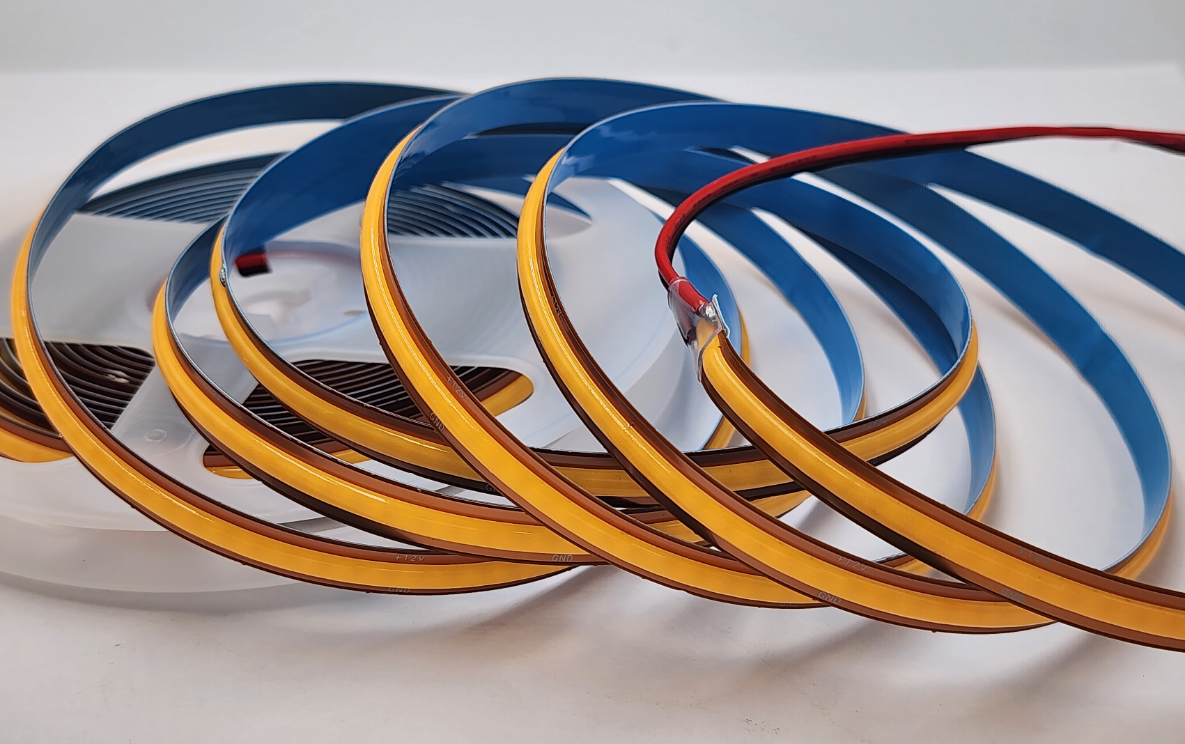
About product
2026年1月12日
An article to explain the different design of the solder pads on led strip
As a buyer/purchaser, some of them even pay attention to the design of the solder pads on led strip.
Solder pads or tinned points (some buyers called it) is a very detailed thing. It's just a difference in design; there's no good or not good in product quality.
Usually there are 4 designs
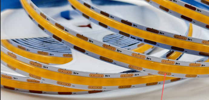
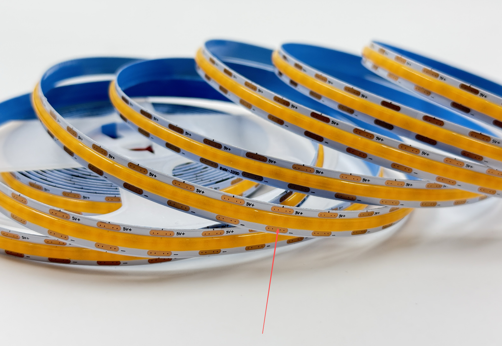
1. On the fron of LED strips. This one is very common.
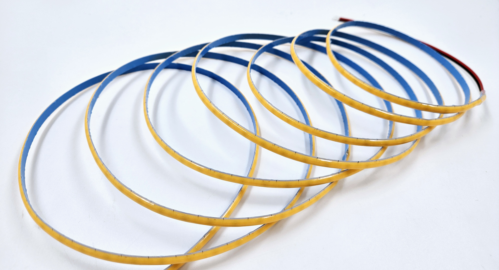
2. On the back of the LED strips so you cann't see the sold pads on the front. Usually it is used for the under 5MM PCB width.
3. No solder pads because PCB itself can conduct electricity. Usually LED strip can cut freely.
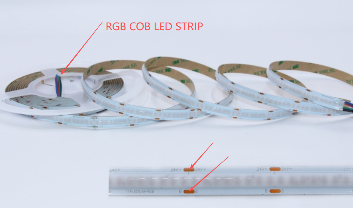
4. Half on the fron of LED strips and half on the back of LED strips. For example,RGB LED strip should be 4 solder pads(+, R,G, B), below is 2 sold pads on the front and 2 sold pads on the back.